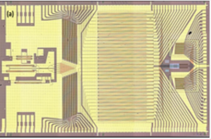
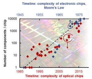
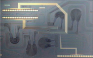
Photonic integrated circuits (PICs) have been growing in complexity with an exponential trend, just like Moore’s Law: the number of components on a PIC doubles every two years. The most well-known PIC technologies are based on silicon nitride, silicon and/or indium phosphide. Different materials have their own strengths and weaknesses. However, for academia and industry, it becomes increasingly impossible to actually fabricate such highly integrated PICs, given the requirements on process yield, quality and reproducibility.
Our unique approach is to work fabless. This means that we work on the theory, the simulations, the design and the experimental characterization of PICs in our Fotonik lab, but the fabrication takes place in (semi-)commercial cleanrooms. This allows us to work on the circuit level, rather than the physical level. By collaborating with mature PIC foundries, our research results have a clear path out of the laboratory, into the real world. We invent to innovate, with a strong focus on performance metrics, to create a competitive technology. Although historically driven by communication requirements, we also explore novel fields for the use of PIC technology.
Communication and Interconnects are currently the main applications of PICs, either in telecommunication or in datacom. We focus our research on energy-efficiency of the overall network. One interesting application, looking far into the future, is the use of photonics for on-chip interconnects. For future electronic-photonic-spintronic integrated circuits, we are designing and realizing experimentally on-chip optical networks that can switch short optical pulses with about a hundred femtojoule-per-bit (100 fJ/b). Although such photonic networks-on-chip (NoC) are still in an infant stage, the research shows that these are far more efficient than electronic NoCs. Our findings can be applied to current interconnect technology too, to drastically reduce carbon footprint of the internet.
Microwave photonics and millimeter-wave photonics are the fields where photonics is used to realize improved technologies for the ~1 GHz – 300 GHz range. Photonics has superior bandwidth, tunability and, in principle, noise performance, as compared to electronics-based technologies. We are using these properties to create ultra-low noise microwave oscillators. Using a combination of silicon nitride PICs and indium phosphide PICs, we intend to achieve this using (coupled) opto-electronic oscillators. These oscillators will, for example, improve the bandwidth of analog-to-digital converters and radars.
Another application is to use PICs for future 5G transmitters, operating at wireless frequencies of 30 GHz and up. We use a single silicon PIC to generate and modulate the carrier and couple this signal to an antenna. Our studies show that our microwave photonics approach consumes less energy than electronic solutions, which means it can be a key enabler for green IoT and 5G networks.
Sensors come in a large variety, and PICs are very promising for some of these. We are currently working on gas sensors, to detect ammonia for future zero-emission agriculture. We do this by scanning a tunable laser over the gas absorption line. A detector then measures the change in laser intensity, which is a measure for the ammonia concentration.
In another project, we are using PICs to realize compact terahertz emitters (300 GHz – 2 THz), by beating two laser frequencies on a photomixer. By making the lasers tunable, we can then achieve tunable terahertz output. These emitters can, for example, be used for stand-off explosives detection and space-based communication.
Past work includes PIC-based Lidar systems, for compact and fast beam steering. Multi-watt output powers, and frame rate beam scanning are, in principle, possible. Such compact and lightweight Lidar systems can find main applications in autonomous cars and drones.