The realm of quantum computing investigates the quantum properties of the physical world, expanding the potential of information processing beyond what classical computers can achieve. Despite their impressive speed and ability to perform specific tasks, quantum computers currently have much smaller sizes compared to classical computers. The main challenge lies in scaling up quantum computers to accommodate hundreds or thousands of qubits without relying on excessively long cables, while maintaining high levels of coherence and achieving low error rates. There is considerable optimism that the development of solid-state quantum computers will eventually lead to scalable architectures, similar to how the invention of the transistor and integrated circuit paved the way for extensive and interconnected classical computers.
CMOS Quantum Integrated Circuits and Systems
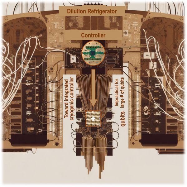
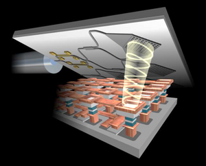
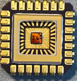
An ideal solution could involve utilizing a CMOS chip, containing billions of transistors, as the basis for a quantum computer with millions of qubits. This solution may involve a CMOS electronic controller located near the quantum processor and operating at cryogenic temperatures. By implementing this approach, the interconnection between components is simplified, and scalability up to thousands of qubits becomes possible. Our primary objective is to develop the electronic interface for quantum devices and quantum sensors. Our work focuses on modeling, designing, and testing cryo-CMOS integrated circuits that are specifically designed to function at extremely low cryogenic temperatures in close proximity to the cryogenic quantum devices.
Spintronic-based quantum computing:
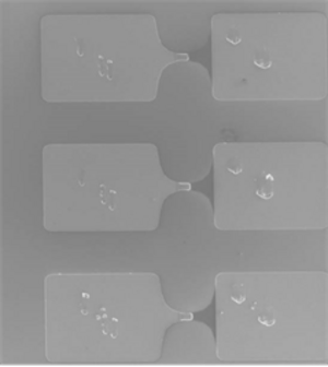
Spintronics is a field of research and technology that focuses on exploiting the intrinsic spin of electrons, in addition to their charge, for various applications in electronic devices. A Magnetic Tunnel Junction (MTJ) is a key component in the field of spintronics, a branch of electronics that utilizes the intrinsic spin of electrons in addition to their charge for various applications. The operation of an MTJ is based on the quantum mechanical phenomenon of tunneling. Quantum tunneling refers to the ability of particles, such as electrons, to pass through energy barriers that would be classically forbidden. In the context of an MTJ, electrons can tunnel through the insulating barrier between the ferromagnetic layers and switch the MTJ state between two stable magnetization states to be used as |0> and |1> in quantum computing. Moreover, there is a possibility to achieve superposition and entanglement quantum states.
Memory is one of the pillar of electronic devices. As such, it has seen decades of research and improvement that has taken it from the few kilobits memory (103 bits) to the now common terabytes hard drives (8×1012 bits). However, microelectronic memories have not been able to increase in performances as fast as computing units mainly because one can generally not increase both the speed and the capacity of a memory at the same time. To compensate this trade-off, a specific memory hierarchy is used in practice. Very fast and very small memories are used near the computing units, because the area is very limited and the data traffic is very intensive. In general, slower but bigger memories are used the farther away they are from the computing units as the area and the data traffic relax. This creates a memory system that « looks » (for the computer) as fast as its fastest memory and as big as its biggest memory. This hierarchical scheme is, however, strongly limited by interconnections speed of metal lines. Several solutions are envisioned, most of them are based on increasing the density of in/near core (aka. very fast) memories so that less out of core (slow) memory space is needed. Another approach is to replace the metal line by photonic connections, which would enable much higher interconnection speed due to the fact that the photonic lines offer a higher bandwidth density and generally much lower losses. These two area each generate a lot of research interests due to the massive scale of the microelectronic industry and the growing part of data handling and storage that arises from the evermore connected world these technologies are creating (see NVM, Photonic: GlobalFoundry, Intel, CEA, IMEC ….).
One of these research interests are the so-called non-volatile memories, they include for commercial example, Hard Drive Disk and Flash memory (USB stick, Solid State Drive, etc.) but also newer technologies like Spin-Transfer Torque magnetic RAM (STT-MRAM). These magnetic memories offer a lot of very interesting characteristics: they are not sensitive to radiation (this is becoming a large problem for very small device), they are generally very robust to working condition, and can be scaled down to nanometric dimensions. However, they are also limited by a trade-off between their retention time (the time they reliably retain the information stored), their energy efficiency, and their speed. In general, increasing one of these characteristics reduces the other. The recent discovery of ultrafast optical switching of the magnetic orientation of a magnetic layer could enable an optical writing for these memories, allowing to break away from this triple trade-off by having a very efficient write at very high speed while keeping their “infinite” retention time intact.
ICELAB, is actively involved in research within memory circuit and architecture design using CMOS and spintronic technology. The relevant works have been published and presented in different Journals and Conferences.
ICELAB is also actively involved in an H2020 FETOPEN project (SPICE) to study the feasibility and potential application of such photonic-spintronic-electronic memory with the objectives of demonstrating the feasibility of the optical switching for an experimental system, and also of developing potential applications and tools to exploit this new concept either at an experimental level or at an industrial level.
Today, the applications for implantable and wearable biomedical systems expands swiftly, which include but not limit to therapeutic and prosthetic devices, Health monitoring systems and body area networks, and tools for neuroscience researches. However, there are still many challenges for reliable, power efficient and body-friendly implementation of such systems. In implantable systems, power and area are severely limited by safety considerations. For instance, tissue-safety standards constrain the thermal losses of an implantable system, as well as the power level of wireless signals to the implanted system(s). For wearable systems, low weight and high power efficiency are highly desirable for the patient's comfort and longer battery lifetime, respectively. These challenges in term of energy and system compactness have provoked interests to develop custom-designed integrated circuits for each specific application. To this end, part of the ongoing researches in the Integrated Circuits and Electronics Laboratory (ICELAB) are focused on application-specific low-area and low-power integrated circuits for implantable and wearable biomedical systems.
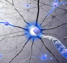
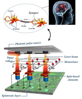
The grand challenge of exascale computing, 1018 operations/second, calls for a dramatic change in hardware of the current petascale supercomputers. With the explosive growth of data on the Internet, 2.5 Exabyte/day and doubling every 40 months, a paradigm shift is required to tackle this issue. A large portion of this data are images and videos; e.g. over 350 million images/day on Facebook and 300 hours of video/minute on YouTube. Such tasks are the most time and power consuming tasks for the existing Von Neumann machines. Due to its massively parallel structure, the brain is capable of doing such tasks in a fraction of second. Recently, neuromorphic computing systems (NCSs) have seen enormous efforts to be a replica for current supercomputer machines by mimicking the parallel processing activity of human brain. However, there still is a huge gap between brain and NCSs in terms of energy consumption and speed. The recent advances in development of spin-based devices integrated with electronics (i.e. spintronics) have opened a door for designers to decrease this gap using spin-based elements. To this end, in the Integrated Circuits and Electronics Laboratory (ICELAB), we are trying to fill this huge gap at different stages including the design of auxiliary circuits, utilizing new spintronic devices, optically assisting the NCS and etc.
In a world with an ever-increasing distribution of electronic devices everywhere, from sensing applications in remote regions of the world, to wearable device embedded in our clothes or carried on our body, they all have one thing in common, they need power to operate. However, Mains and batteries are not applicable for powering them, all the times. Mains might not be available in remote areas of the world, and they may cause infections for an implantable device. Battery is a decent option that gives the possibility of mobility, but battery lifetime is a limiting factor, and swapping them out might not be feasible or even possible. Energy harvesting is an alternative solution, where energy needed for a given application is harvested directly from the surrounding environment.Examples of this are solar-cells which are based on the photovoltaic effect of converting light to electrical energy, thermo-electric generators (TEG) which can generate power if there is a temperature difference across them, and piezoelectric crystals which can generate electric power when mechanically vibrated with ultrasonic waves. One ongoing specific topic of research in ICELAB, is using sub-mm sized piezoelectric crystals as a means of harvesting ultrasonic power for miniaturized optogenetic neural stimulators implanted deep in the brain.