1. Metamaterials / metasurfaces
Metamaterials / Metasurfaces are artificial 2-dimensional arrays of subwavelength unit structures. They can be used to manipulate electromagnetic waves across the spectra, i.e., from UV, visible, infrared, THz to microwaves, and can control wave amplitude, phase, polarization, angular momentum. Previously, we have demonstrated that thin film metamaterials can work as THz filters, phase shifters, waveplate and lens. We continue the research activities on metamaterials / metasurfaces for optical devices.
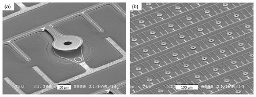
2. MEMS / NEMS controlled dynamic metasurfaces
MEMS is short for micro-electro-mechanical systems (NEMS for nano-electro-mechanical systems). MEMS / NEMS devices with electrostatic actuation have advantages of small footprint, low power consumption, and electrical signal control. By combing MEMS / NEMS techniques with metasurfaces, we can obtain dynamic metasurfaces, where the dynamic mechanism comes from the structure reconfiguration, which intrinsically inherits the merits of MEMS electrostatic actuation. By scaling the device sizes, it is promising to have high speed modulation, up to GHz.
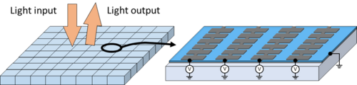
3. Spatial light modulators (SLM)
Spatial light modulators (SLM), an array of modulators, is a device that can spatially control light intensity, phase, or polarization. These devices are used in applications such as holographic displays, augmented reality (AR), and bio-imaging, that require dynamical shaping of the light beam. Based on MEMS / NEMS metasurfaces, one can straight forward to configure an SLM with an array of light modulators, where thanks to the varieties of metasurface functions, it is promising to achieve all these (intensity, phase, polarization) SLM devices. With scaling down the device size, one could obtain high speed SLM.
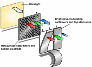
4. Novel optical displays
Optical displays play a ubiquitous role in daily life, being an essential component of smartphones, computers, televisions, etc. However, these devices make up roughly half of the 50 million tons of e-waste produced globally every year. There is an urgent need for alternative display technologies which are easier to recycle and are financially feasible to be incorporated into sustainable consumer electronics.
We propose a new type of optical display technology based on MEMS and metasurface aiming to solve the e-waste problem. The proposed technology combines MEMS micro cantilevers and metasurface artificial designed structures colours to realize full range RGB displays, while the devices use only few common earth-abundant and environment friendly materials, potentially able for cost effective products and ultra-fast optical display.
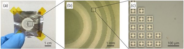
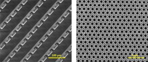
5. Micro-nano fabrication
Modern electronics have renovated our life and society, where the core is semiconductors. In our group, we study and employ micro-nano fabrication technology, such as lithography, etching, and deposition, etc., to build miniaturized devices or systems for applications in optics, electronics, and more.
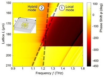
6. Extreme metasurfaces (spectral phase singularity)
Optical phase manipulation can bring advantages for information technology, such as enabling holography and polarization encryption. In general, when light amplitude comes to zero from reflection or transmission or absorption, phase has rapid change. One example is that at the Brewster angle with reflection coefficient of zero, the phase of the reflection wave has sharp change. In our group, we try to design and demonstrate with metamaterials / metasurfaces to realize such sharp phase change, which in other words is called spectral phase singularity.